Project information:
(1) The minimum size of the wafer/wafer is 4 inches, and the grain/die size on the wafer is 250 * 256um. A wafer is divided into 10 BT (Blue tape) sheets, and visual inspection is conducted in BT units.
(2) The upper and lower camera systems take images simultaneously, achieving unified relationship and appearance inspection of the positive and negative surfaces of the wafer/grain.
(3) A maximum of 40 (5 * 8) grains can be detected in one image, with a theoretical pixel accuracy of 0.7um.
(4) Traditional manual inspection only detects the front side, with a rhythm of 1K-2K grains per hour. Due to the fatigue caused by visual inspection, misjudgment is prone to occur after long-term work; Due to the boredom of testing work and the inconvenience of the wafer dust-free workshop, the turnover rate of testing personnel is relatively high. Zhenyoudao's wafer AOI visual inspection system can detect up to 11K grains per hour at a maximum beat, with a leakage rate of less than 0.5%.
Difficulties:
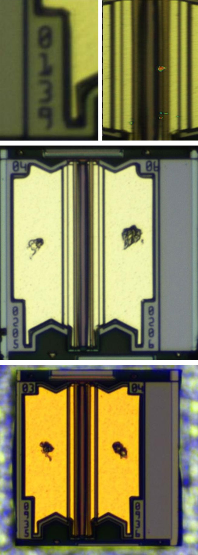
(1) The same specifications or even grains on the same BT will have color and structural differences caused by the process, which poses challenges to the applicability and stability of visual algorithms, and traditional algorithms cannot achieve applicability.
(2) There are normal probe marks (similar to dirty features) in the grain solder pad area, and there may be differences in the number and shape of probe marks with different wafers, which makes traditional algorithms unable to achieve defect detection in this area.
Testing requirements:
(1) Front: The print number above and the serial number below interact with CSV data and read electrical measurement values.
(2) Front: The width of the upper and lower terraces and defects such as dents, dirt, and defects on the upper steps.
(3) Front: The width of the left and right terraces is affected by dirt, defects, cracks, and other defects.
(4) Front: Defects such as delamination, dirt, pits, defects, and pressure damage on the surface of the luminous strip, upper and lower light outlets.
(5) Front: Detection of dirt, scratches, etc. in key areas of the solder pad, and detection of probe damage at the edge of the solder pad.
(6) Front: Abnormal color and dirt on the overall surface.
(7) Negative side: Overall size, poor cutting.
(8) Summary: Based on the use of artificial intelligence deep learning algorithms combined with traditional visual algorithms, this system can effectively detect relevant types of defects and achieve the required rhythm and accuracy requirements.
Summary: Based on the use of deep learning algorithms using artificial intelligence, combined with traditional visual algorithms, this system can effectively detect relevant types of defects and achieve the required rhythm and accuracy requirements.

 中文
中文 ENG
ENG